

 English
 中文
中文What Are You Looking For?
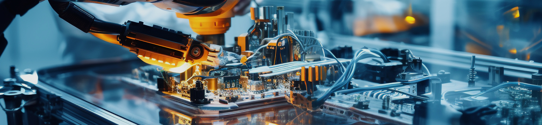
At Midea Electronics, quality isn't just measured—it's seen, scanned, and decoded. Tucked within our comprehensive ecosystem of 7 specialized labs and 3 functional zones, the Failure Analysis Laboratory serves as our diagnostic command center, where we uncover hidden flaws and turn failure into foresight.

The Failure Analysis Lab: Your Diagnostic Partner
When a PCBA fails—whether at your facility, ours, or in the field—we don’t guess. We investigate. From BGA soldering quality and component breakdowns to complex root-cause analysis, this lab delivers the clarity needed to reduce risk, improve yields, and protect your reputation.
Meet the Detectives: Our Precision Equipment with Personality
Ultrasonic Scanning Microscope | Crestwave SAM301
Think of it as the device with “X-ray vision” for semiconductors. It scans with micron-level precision—from a tiny 1μm² to a broad 320mm²—to spot hidden flaws like delamination, cracks, or tilted wafers. All without a single scratch.
High-Resolution X-Ray | YXLON Cougar evo
Our silent observer. With 1.5μm resolution and 100nm feature detection, it peers deep into PCBs and components, revealing inner structures at up to 10,000x magnification. No disassembly required.

Laser Decapsulation System | GLASER Smart Etch Ⅱ
The gentle surgeon. Using a finely tuned 40μm laser spot, it carefully uncaps even the most delicate IC packages—exposing the core for inspection while keeping functionality intact.
What Happens Inside?
Destructive Physical Analysis (DPA): From encapsulation, cutting, and polishing to morphology and composition analysis
Non-Destructive Inspection: Using ultrasound and X-Ray to see inside without damage
3D Profilometry: Measuring flatness and warpage of BGA assemblies
Laser & Chemical Decapsulation: For precision access and optical inspection

More Than One Lab: A Full Ecosystem of Excellence
The Failure Analysis Lab is one key part of Midea’s integrated quality backbone—7 advanced labs + 3 functional zones—covering everything from signal integrity and environmental testing to materials validation and EMI/EMC compliance. Together, they form one of the most capable electronics validation hubs among EMS providers.
Why This Should Matter to You
In a world where failures cost more than money—they cost trust—we provide:
Faster root-cause analysis and resolution
Enhanced product reliability and lifecycle performance
Confidence backed by full-spectrum testing capabilities
You can’t improve what you can’t see. With Midea, you see everything.
Ready to work with a partner who leaves nothing to chance?
Let’s build with confidence. DM us or visit midovax.com.